What the Project Is About
At its core, this project focuses on developing anisotropic thermal interface materials designed specifically for cooling high-powered, complex, and compact electronics. The goal? To tackle one of the most critical challenges in modern electronics—efficient thermal management. HYMET introduces a new category of thermal interface materials (TIMs) that come with integrated deformable heat spreaders. This isn’t just another product; it fills a unique gap in the market, addressing a foundational need in the semiconductor industry that has often been overlooked.
Main Benefit of the Project
The benefits of this innovative approach are clear and impactful:
- Increased reliability of electronic devices
- Enhanced performance under demanding conditions
- Extended longevity of electronics, meaning devices last longer
- Reduced power consumption, which is great for energy efficiency
- Lower manufacturing costs, making advanced cooling more accessible
- Decreased rate of e-waste entering landfills, supporting environmental sustainability
Why Thermal Management Matters
Thermal management is absolutely crucial in electronics, especially as devices become smaller yet more powerful. Without effective heat dissipation, components can overheat, leading to failures or reduced performance. HYMET’s materials address this by offering a solution that adapts to complex geometries and compact spaces, ensuring heat is spread and dissipated efficiently. This means devices can run cooler, safer, and longer—pretty important stuff in today’s tech-driven world.
Innovative Material Design
The project’s standout feature is the integration of deformable heat spreaders within the TIMs. This design allows the material to conform to irregular surfaces, improving contact and heat transfer. It’s a clever approach that combines flexibility with high thermal conductivity, something that traditional materials often struggle with. The result? A thermal interface that’s not only effective but also versatile enough for a wide range of electronic applications.
Environmental and Economic Impact
By improving thermal management, the project indirectly contributes to reducing electronic waste and energy consumption. Longer-lasting electronics mean fewer replacements and less waste. Plus, lower power consumption translates to less strain on energy resources. Economically, the reduced manufacturing costs can make advanced cooling solutions more affordable, potentially driving wider adoption across industries. It’s a win-win for both the planet and the market.
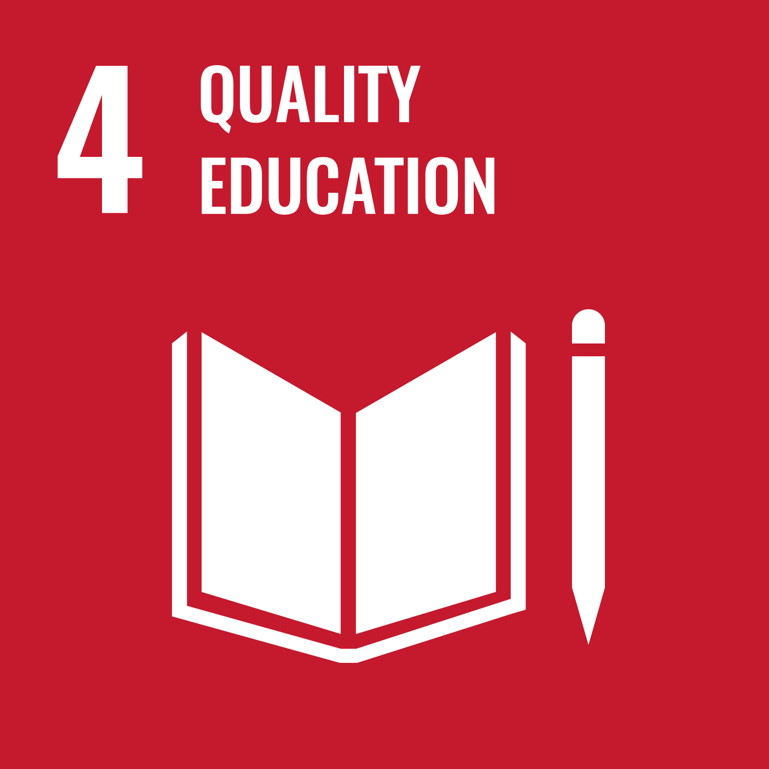
Project Impact on Sustainable Development Goals (SDGs)
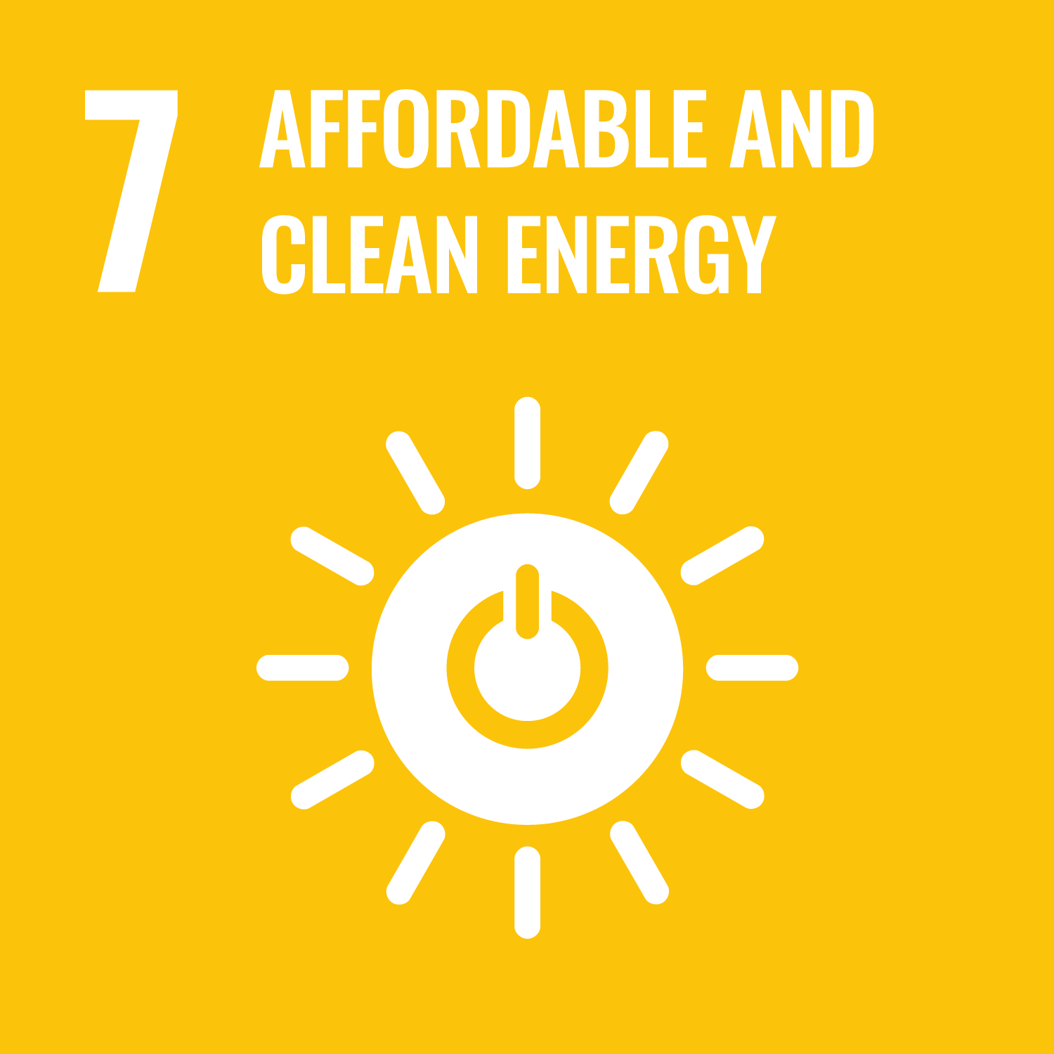
- SDG 7: Affordable and Clean Energy – through reduced power consumption
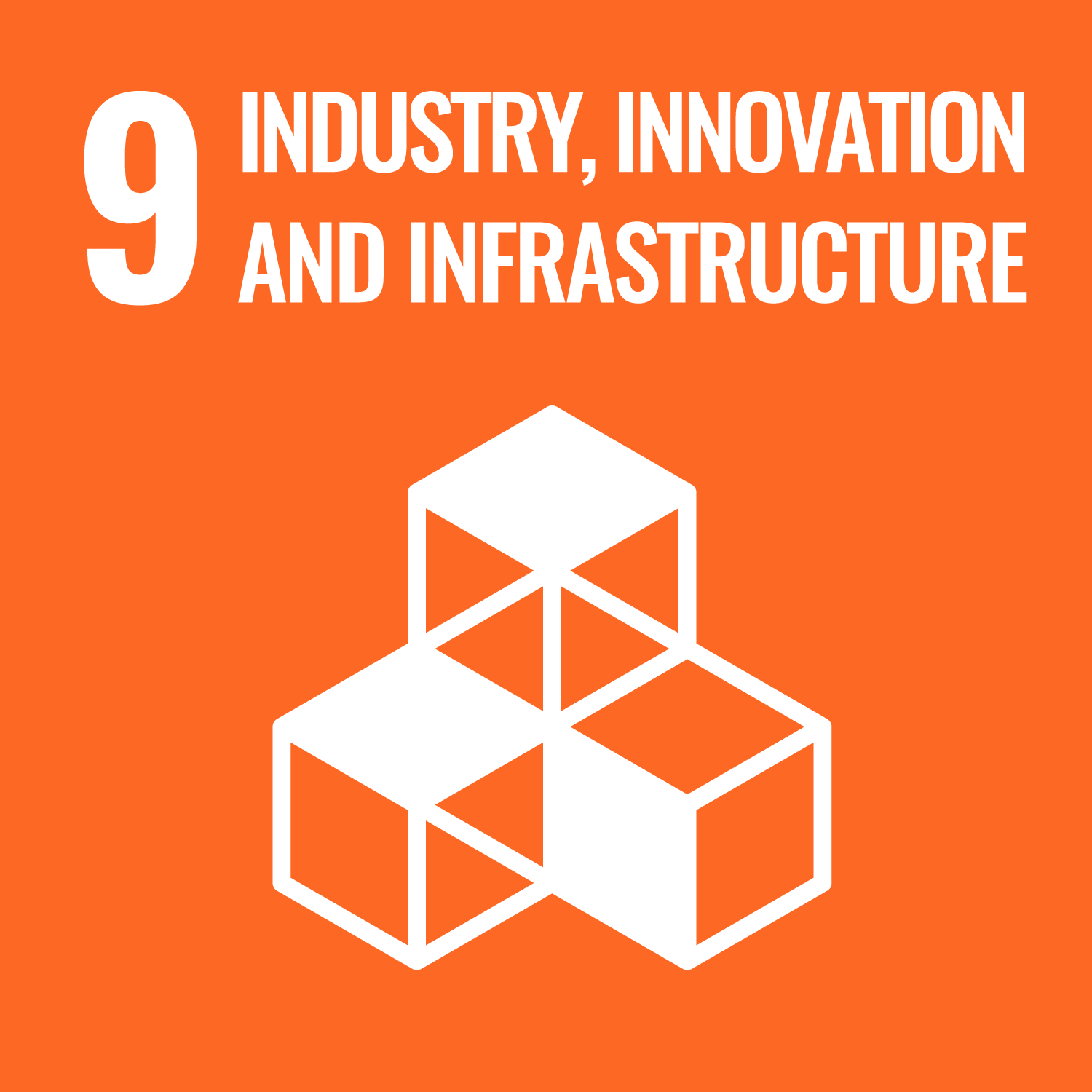
- SDG 9: Industry, Innovation, and Infrastructure – by advancing semiconductor technology
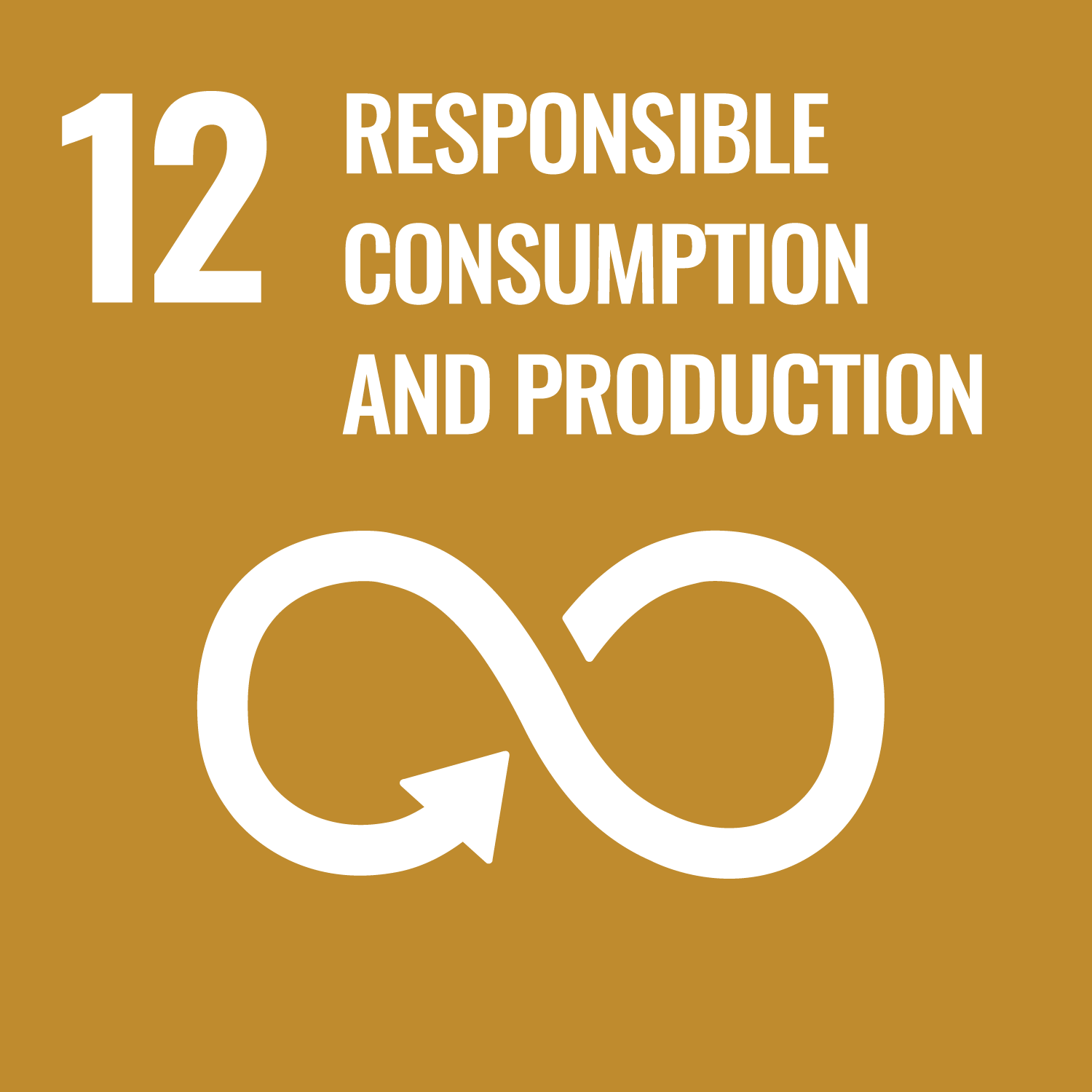
- SDG 12: Responsible Consumption and Production – via decreased e-waste
- SDG 13: Climate Action – supporting energy efficiency and sustainability
Looking Ahead
The HYMET project is setting a new standard in thermal management for electronics. As devices continue to evolve, the need for smarter, more adaptable cooling solutions will only grow. This project not only meets today’s demands but also paves the way for future innovations in the semiconductor industry. It’s an exciting step forward—one that promises to keep electronics cooler, more reliable, and kinder to the environment.